About us
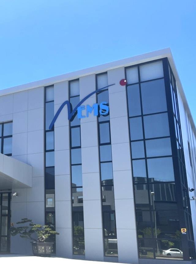
About Us
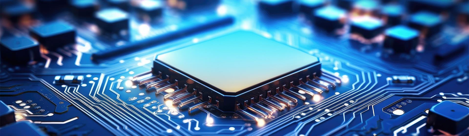
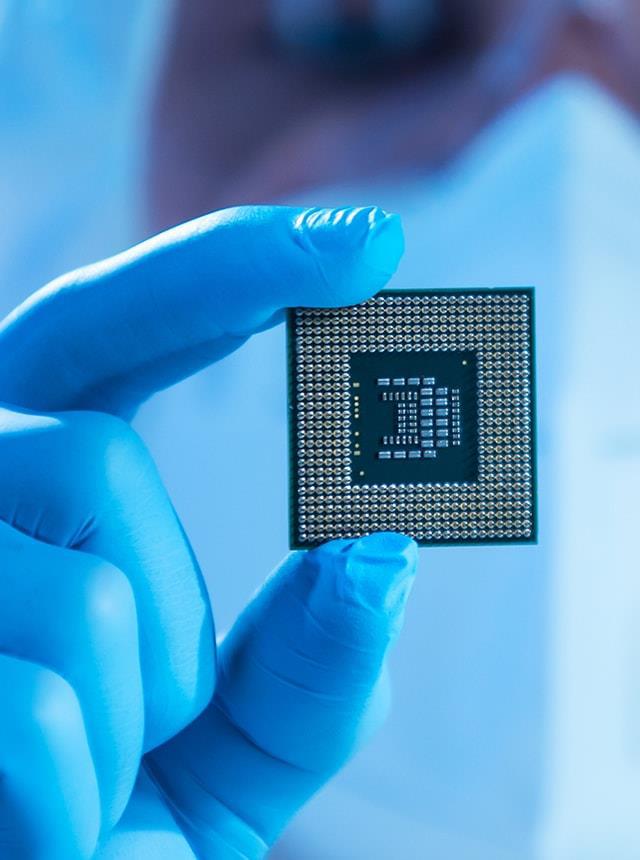
Nano Electronics and Micro System Technologies, Inc., founded in 2002, is a leader in plasma technology innovation, providing high-performance surface treatment solutions across industries like semiconductors, PCBs, and optoelectronics. With a strong R&D team, we've secured multiple patents in high-density ICP and atmospheric plasma technologies, serving markets in Japan, the U.S., and Europe.
Our core strengths lie in continuous innovation and excellence, extending beyond electronics to consumer industries and biomedicine. We value integrity, cooperation, and a ‘family culture’ that nurtures employee growth and fosters a sense of belonging.
Committed to continuous improvement, we strive for excellence in every aspect of our operations. Looking forward, we aim to lead in technology while contributing to societal and economic advancement through our innovative products and global partnerships.
Business Philosophy
NEMS’ success is driven by its commitment to innovation, excellence, integrity, cooperation, family culture, and continuous improvement.
Innovation and Excellence
NEMS’ focuses on innovation and product quality, investing in R&D to stay industry-leading. Excellence in customer service and product development ensures long-term partnerships and mutual success.
Integrity and Cooperation
The company values integrity as the foundation of all business practices, fostering transparent relationships with customers, suppliers, and employees. This approach builds lasting trust and cooperation.
Family Culture
NEMS’ treats its employees as its greatest asset, offering a supportive work environment that encourages personal and professional growth. This culture boosts employee satisfaction, loyalty, and team creativity.
Continuous Improvement
NEMS’ is dedicated to continuous improvement, optimizing processes, products, and strategies to stay ahead in a competitive market.
Together, these principles guide NEMS’ in its mission to achieve business excellence, uphold social responsibility, and create lasting value for shareholders, employees, and society.
Company Development History
NEMS Foundation
- Established a technical team centered on plasma technology, developing various plasma equipment and initially focusing on semiconductor packaging applications.
- Started venturing into the PCB field, developing plasma etching machines, making the technical team the first in the country to develop this equipment successfully.
- In June, Nano Electronics and Micro System Technologies, Inc. was established in response to the addition of strategic partners and new investors.
- Collaborated with IC substrate manufacturers to develop a Plasma Driller for unique patent processes in IC substrates. This application resolves technical bottlenecks encountered with laser drilling machines in the process.
- Started venturing into the optoelectronics field, developing Plasma Cleaning Machines for LCM in LCD processes, with sales reaching 40 units in the same year. Simultaneously, the full-scale development of atmospheric pressure plasma technology began in the latter half of the year.
- We have successfully developed a variety of atmospheric pressure plasma cleaning machines for LCD and PCB applications, including waterfall, matrix, and jet types. The jet type includes both high-frequency and low-frequency variants.
- Completed the development of continuous plasma cleaning machines.
- Applied various atmospheric pressure plasma devices to consumer industries such as the plastics and automotive lighting industries.
- Successfully applied plasma technology for the first time in biomedical sciences.
- Started selling plasma equipment to the manufacturing sector of touchscreen displays.
- Developed applications in plasma sterilization, waste gas treatment, and air purification.
- Obtained plasma equipment certification from a leading semiconductor manufacturer in the United States, and successfully sold plasma equipment to the U.S.
- Introduced plasma technology into the golf and textile industries, addressing bottlenecks and limitations in traditional processes.
- Initiated the research and development of atmospheric pressure plasma coating technology.
- Successfully developed continuous plasma decapsulation machines and roll-to-roll plasma decapsulation, leading the industry and selling them to major PCB manufacturers.
- Formed a strategic alliance with the Japanese super equipment manufacturer, Company H, and began mass sales of plasma equipment to leading customers in various electronic industries in Japan, opening a new chapter in sales in the Japanese market.
- Sold surface coating equipment to touchscreen and optical component industries.
- Conducted customer certifications for atmospheric pressure plasma equipment in shoe industry applications, and successfully sold related plasma machinery.
- Ventured into the solar energy industry application and successfully sold innovative atmospheric pressure plasma systems.
- In response to the transformations and demands of Industry 4.0, we have developed various production line monitoring systems.
- Successfully introduced plasma technology into the application of 5G mobile phone antenna supply chain, and extensively applied plasma machinery in the processes of high-frequency materials such as LCP.
- Ventured into the European market, adding a new chapter to NEMS’ cutting-edge plasma technology.
- Developed unique plasma polarization technology, successfully applied this technology to the manufacturing process of under-screen fingerprint recognition chips for 5G smartphones, and obtained plasma equipment certification from a leading semiconductor manufacturer in the United States.
- The advanced high-temperature plasma torch technology development has been completed. It is now being applied to treating of solid waste and waste oil, providing an excellent solution for environmental protection and waste reduction.
- Sold various high-performance plasma etching machines (including microwave plasma etching machines and reactive ion etching machines) in the wafer and IC substrate manufacturing fields, especially for etching various polymer materials or metals.
- Obtained plasma equipment certification from a leading semiconductor giant in Taiwan, initiating sales and collaboration relationships for the group.
- Providing several plasma solutions for wafers, including wafer regeneration, plasma wafer cutting, and wafer thinning, continuously obtaining customer certifications.
- Fully committed to developing various plasma energy-saving and carbon reduction solutions and initiating the Plasma Creating Clean New Energy project to provide new strategic solutions for sustainable business (ESG).
- Pioneering advanced plasma technology to build a global leadership brand.