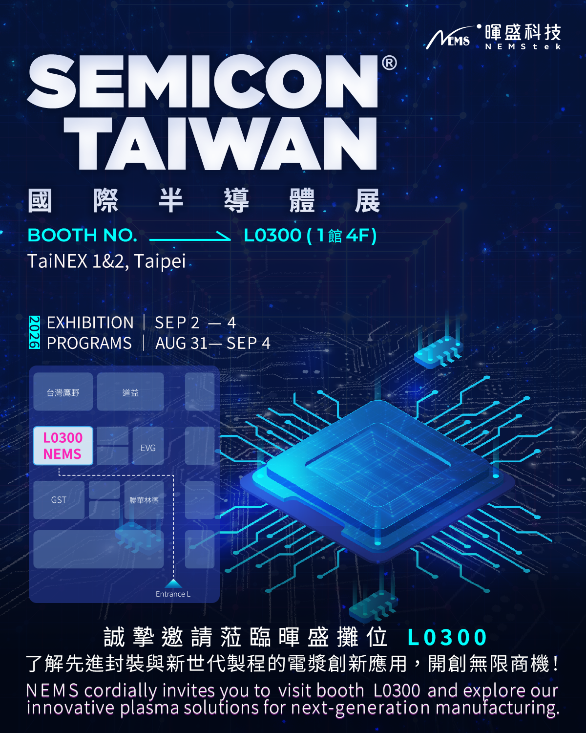
NEMS Showcases 8 Advanced Plasma Technology Focus Areas at SEMICON Taiwan 2026
NEMS will showcase its latest plasma technologies and applications atSEMICON Taiwan 2026, focusing on glass substrates, advanced packaging, silicon photonics, wafer processes, and green manufacturing, demonstrating the value of plasma technology in next-generation semiconductor manufacturing.
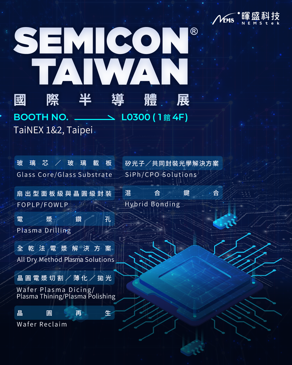
8️⃣ Key Technology Focus Areas
1. Glass Core/Glass Substrate
Glass materials offer low warpage, high dimensional stability, and excellent high-frequency signal transmission characteristics, making them an increasingly important material for next-generation packaging. NEMS will showcase plasma process solutions for glass material processing, surface modification, and subsequent metallization.
2. FOPLP/FOWLP Fan-Out Panel-Level and Wafer-Level Packaging
For Fan-Out Panel-Level Packaging (FOPLP) and Fan-Out Wafer-Level Packaging (FOWLP), NEMS utilizes highly uniform and stable plasma activation and cleaning technologies to improve material adhesion and process interface quality, enhancing packaging reliability.
3. Plasma Drilling
Plasma drilling technology can be applied to ABF substrates, glass substrates, and advanced packaging processes, providing high-precision, low-damage microfabrication capabilities to meet the requirements of high-aspect-ratio and high-density structures.
4. All Dry Method Plasma Solutions
By replacing some wet chemical processes with plasma technology, NEMS helps reduce chemical consumption and wastewater discharge while improving process stability, addressing the needs of green manufacturing and ESG.
5. Wafer Plasma Process
NEMS will showcase wafer plasma applications including Wafer Plasma Dicing, Wafer Plasma Thinning, and Wafer Plasma Polishing, supporting process requirements for wafer dicing, thinning, and polishing.
6. Wafer Reclaim
Through plasma processes for wafer surface treatment and reclaim, NEMS helps improve wafer reuse efficiency, supporting material efficiency and cost management in semiconductor manufacturing.
7. SiPh/CPO Silicon Photonics and Co-Packaged Optics
In response to the demand for high-speed data transmission in AI data centers, NEMS will showcase plasma surface treatment solutions for SiPh/CPO, helping improve material adhesion, interface cleanliness, and component reliability.
8. Hybrid Bonding
To meet the requirements of Chiplet, 3D IC, and heterogeneous integration, plasma surface activation and cleaning can improve bonding interface quality, enhance bonding strength, and reduce the risk of process defects.
From glass substrates and advanced packaging to silicon photonics, co-packaged optics, and wafer processes, NEMS continues to deepen its plasma technology and equipment development, expanding the applications of plasma processes in next-generation semiconductor manufacturing.
🙌 Welcome to visit NEMS at Booth L0300 during SEMICON Taiwan 2026 and connect with us.
Exhibition Information
Exhibition Dates| September 2 (Wed.) to September 4 (Fri.), 2026
Exhibition Hours| September 2–3, 10:00–17:00; September 4, 10:00–16:00
Venue| Taipei Nangang Exhibition Center, Hall 1, 4F
NEMS Booth| L0300