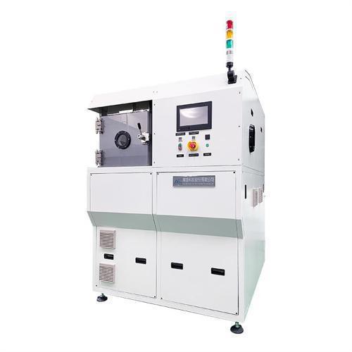
Product
NEMST-RIE2018系列
Reactive Ion Etching Plasma Machine
- Patented High-Density ICP Plasma Source: ~ion density about 1011~1013/cm3.
- Single-side treatment in 1 cycle.
- Unique Distribution Panel Design is employed to ensure uniform plasma generation.
- The bias (DC Pulse or RF) is applied to the product holder.
- An adjustable electrode gap is available.
- Big Area RIE is available.
- End Point Detection is available.
- The system can be configured to a pure ICP source for remote plasma application.
- Achieve anisotropic/high aspect ratio etching. Based on customers' requirements, 6" wafer, 8" wafer, 12" wafer and even 660 mm x 660 mm panel can be well conducted. Fast etching by radicals or ions. Very high treatment uniformity. (93% or Above in general) Can produce high-density plasma at low pressure.
- Plasma density and bias can be controlled independently.
- Suitable for etching Polymer Material (Polyimide, Parylene, FR4, BT, Teflon, etc.), Silicon, Passivation (Si3N4 or SiON), Dielectric (SiO2, High-K, Low-K, etc.), Semiconductor Compound (GaN, GaAs, InP, SiC and etc), Metals (Al, Ti, Metal Alloys and etc), Other Material (Sapphire, Diamond, ITO, PZT, etc.). Employed for Processes of Semiconductor, Advanced Packaging (Wafer-Level Packaging, Panel-Level Packaging, 2.5D/3D, CoWoS), IC Substrate, Mirco-LED, Wafer Reclaim, and etc.